
The Next Generation in Semiconductor Decapsulation and Etching
Atmospheric pressure die-level etching of inorganic and organic materials without ion bombardment.
Breakthrough Innovation in IC package decapsulation
Automated atmospheric pressure Microwave-Induced-Plasma (MIP) decapsulation.
What is Microwave Induced Plasma (MIP) decapsulation?
MIP (Microwave Induced Plasma) decapsulation is a technique used to remove the encapsulating material from integrated circuit (IC) packages, allowing for failure analysis and access to the underlying chip and wire bonds. It utilizes atmospheric pressure plasma with oxygen and patented hydrogen-based recipes, offering advantages over conventional plasma etching methods.
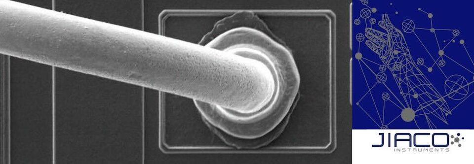
MIP decap is a method to remove the encapsulant (e.g., glob-top, underfill) from IC packages without damaging the die, wire bonds, or critical structures.
The IC decaping using MIP allows engineers to examine the chip and its connections for failure analysis, reliability testing, qualification, or cybersecurity.
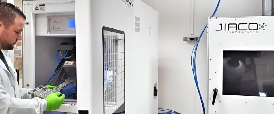
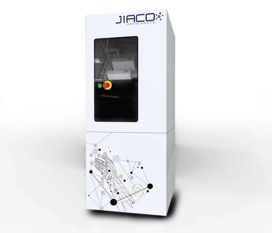
JIACO Instruments is a company known for developing Microwave Induced Plasma and providing MIP decapsulation systems to failure analysis and reliability labs.
How does MIP work?
Chemical Radicals
MIP decapsulation uses a microwave-induced plasma to create chemical radicals for isotropic etching.
Oxygen and Patented Hydrogen Recipes
This plasma is generated using oxygen and a patented hydrogen-based recipe, ensuring minimal damage to the IC components.
IC Package Decap
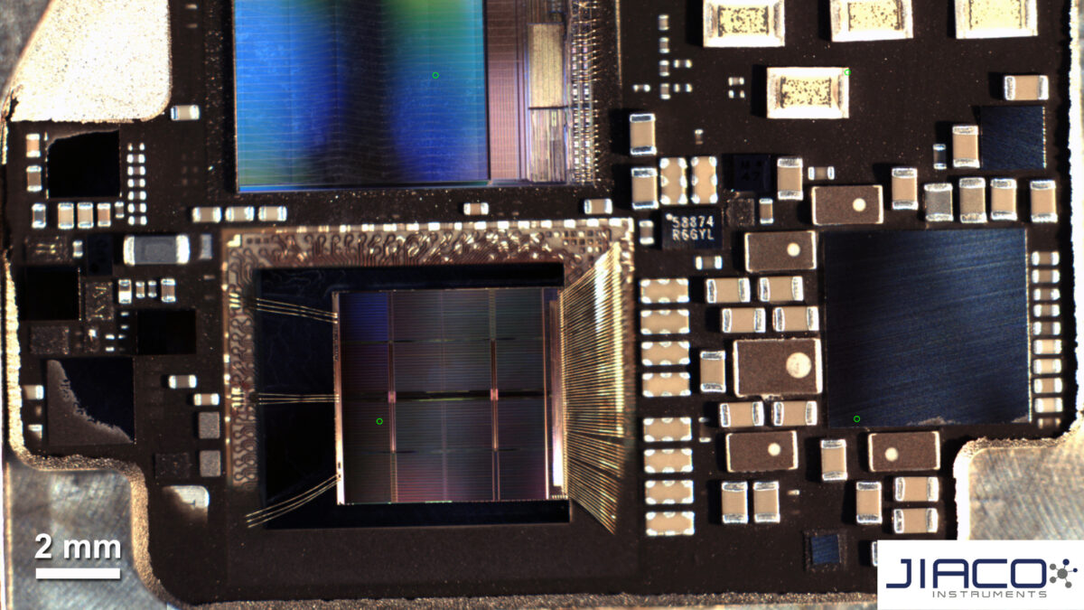
It is particularly effective for decapsulating complex IC packages like 3D, SiP, and BOAC devices, among others..
Advantages of MIP Decapsulation
Preserving Critical Structures
MIP decapsulation avoids the overetching damage caused by conventional plasma etching methods, especially when dealing with thin copper metallization traces on passivation.
Rapid Sample Preparation
The process is efficient and allows for quick access to the area of interest during failure analysis.
Minimizes Artifacts
MIP decapsulation helps avoid the introduction of artifacts that could contribute to uncertainty in the fault detection process.
Versatile
It's suitable for various IC packages and wire bond types, including Cu, PCC, Ag, and Au.
Applications for MIP
Failure Analysis
Failure analysis of ICs.
Reliability Testing
Reliability testing of ICs.
Qualification
Qualification procedures for new processes and materials.
Cybersecurity
Recover lost data, test vulnerabilities.
Our Microwave Induced Plasma (MIP) Systems
MIP | IC Decapsulation
Automated atmospheric pressure MIP IC decapsulation utilizing only Oxygen and patented Hydrogen-based recipes. MIP is the global standard for tackling the semiconductor industry’s most demanding decapsulation challenges.
Learn More
Learn More
MIP+ | Die-level Etching
The Next Generation in Semiconductor Decapsulation and Etching. MIP+ extends MIP’s proven capabilities from package-level to die-level etching.
Learn More
Learn More