
MIP+ | Plasma Die-level Etching
A breakthrough innovation that extends MIP’s proven capabilities from package-level to die-level etching. Developed in collaboration with leading advanced packaging users, MIP+ redefines etching technology. Request information
New Etching Chemistries
Localized, ion-free solutions for Si, SiO₂, Si₃N₄, and more.
Unparalleled Versatility
Atmospheric pressure etching of inorganic and organic materials without ion bombardment.

Cutting-Edge Performance
Selectively etches advanced packaging and die materials, while preserving critical underlying features.

Expanded Applications
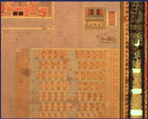
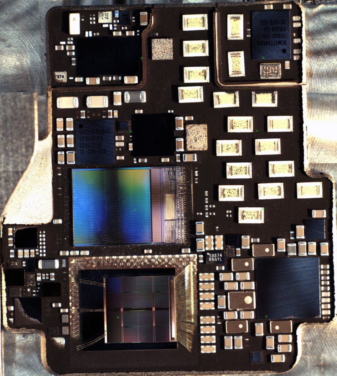
Localized selective etching of die materials for sample preparation for analysis on 2.5D and 3D packages, interposer die, memory die, advanced node Si die, compound semiconductor die.
Package-Level + Die-Level Capabilities
MIP+ enables decapsulation and etching of both packaging and die structures, ensuring deeper insights into semiconductor designs.
Proven Reliability
Built on the success of MIP’s localized, ion-free etching approach, which has been globally recognized in industry publications and incorporated into standards such as JEDEC JESD22-B120.